


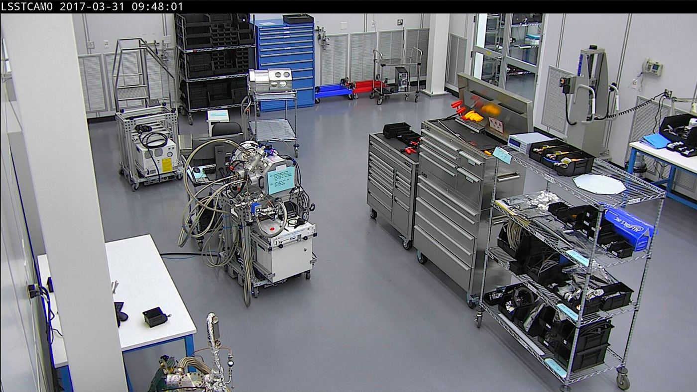
Making computer chips is thirsty work. Semiconductor factories rinse wafers repeatedly in ultrapure water, water stripped of almost every dissolved mineral and particle, and a large plant can use as much each day as a small city. That dependence has become a strategic concern in regions where chip production is expanding faster than local water supplies. In response, manufacturers are investing heavily in recycling systems that capture rinse water, remove traces of chemicals and metals, and return it to production at the required purity. Modern plants report reclaiming the great majority of their process water, with separate treatment streams for different contaminants so that lightly used water is cheap to restore while heavily contaminated flows receive intensive processing. Engineers monitor recycled water continuously, because a single purity failure can ruin batches of wafers worth far more than the water itself. The result is a factory within the factory: kilometres of piping, filtration membranes and sensors dedicated to keeping water circulating rather than discharged.
What the Evidence Shows
Recycling at this scale changes both the economics and the politics of new chip plants. Communities asked to host factories increasingly scrutinise water demands during drought planning, and demonstrably high recovery rates make approvals easier to win and keep. Technology suppliers have responded with modular treatment systems designed for the particular chemistry of chip making, including silica, fluoride and the solvents used in patterning. There are limits, however. Each recycling loop consumes energy and produces concentrated waste that still needs safe handling, so engineers optimise for overall impact rather than chasing the final few percent of recovery. Factories are also pairing recycling with rainwater capture, partnerships with municipal treatment plants and real-time reporting of withdrawals, building a fuller picture of their water footprint. As governments subsidise domestic chip production, water performance is becoming part of what a state-of-the-art fab means. The cleanest room in manufacturing now depends on proving that its invisible water systems are as advanced as its lithography. Reporting and analysis from sources such as Wired track the same developments, and specialists following ultrapure water recycling inside semiconductor factories say the direction is now consistent across independent lines of evidence.
The Wider Context
The wider context is an industry learning to ship capability and restraint together. Products built around ultrapure water recycling inside semiconductor factories now launch with safety evaluations, usage data and rollback plans as standard, because enterprise buyers and regulators ask for them in the first meeting. Companies that treated those questions as friction are discovering they have become the purchase criteria.
What Happens Next
What happens next for ultrapure water recycling inside semiconductor factories depends less on another breakthrough than on the unglamorous work of reliability, pricing and support. The buyers evaluating it now are not enthusiasts; they are operators with budgets and auditors, and their checklists will decide the timeline. On the evidence of the current pilots, the technology has earned the right to be judged by them. You can follow related developments in our coverage of technology.
None of this will be settled by a single announcement, study or product launch. The pattern to watch is accumulation: independent confirmations, honest reporting of failures and steady improvement in the underlying numbers. Readers who follow those signals, rather than the loudest claim of the week, will understand this subject better than most of the commentary surrounding it suggests is possible.
